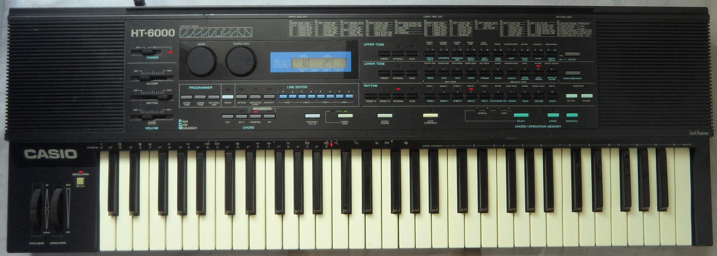
hardware details
The Casio HT-6000 is derived from the HT-3000
hardware family (see there) but is much more complex. It is built around
the CPU NEC D78C10G that controls
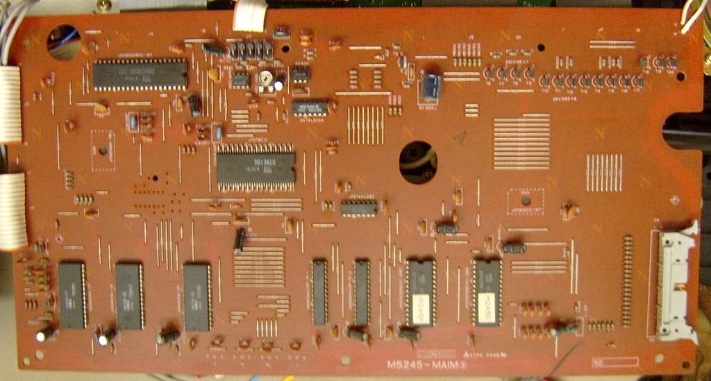
here 4 SD sound ICs NEC D935G and 3 percussion
ICs OKI M6294-07, -08 and
-09. Each sound IC has 2 VCA JRC 2090D
attached, those outputs can be routed to upper or lower (chord) channel.
The upper channel goes through the stereo chorus. 2 of the sound ICs control
the LCD. Keyboard velocity sensing uses a key controller M6200
that is handled by a separate CPU NEC D80C49HC-187.
Bus data latching and control panel matrix use 2 gate array ICs.
This hardware analysis is based on a Casio HT-6000 service manual PDF and
others from related HT-3000 hardware.
Also here the CPU is contains no firmware but uses only external rom;
custom chips (beside percussion ICs) have no software numbers, so unless
it hides something nasty inside its gate arrays (those officially only
latch and demux buses), this makes the system open for experiments with
custom software by replacing the roms with socketed 32KB eproms (27C256)
to change preset sounds or (more interesting) implement proper midi sysex
dump support to get rid of the rare ram cards and define synth parameters
though midi.
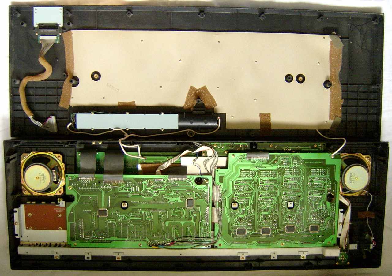
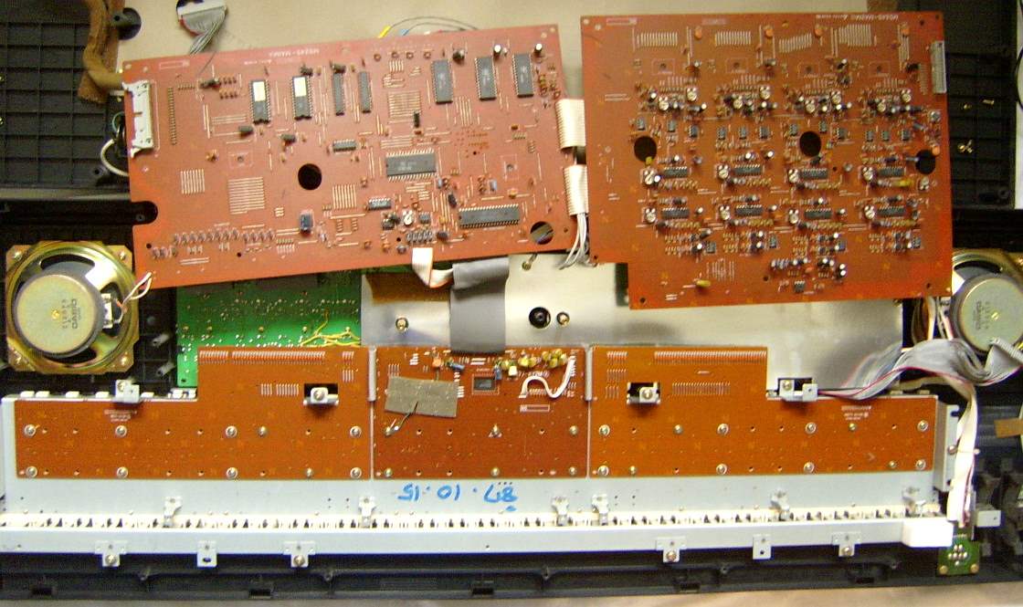
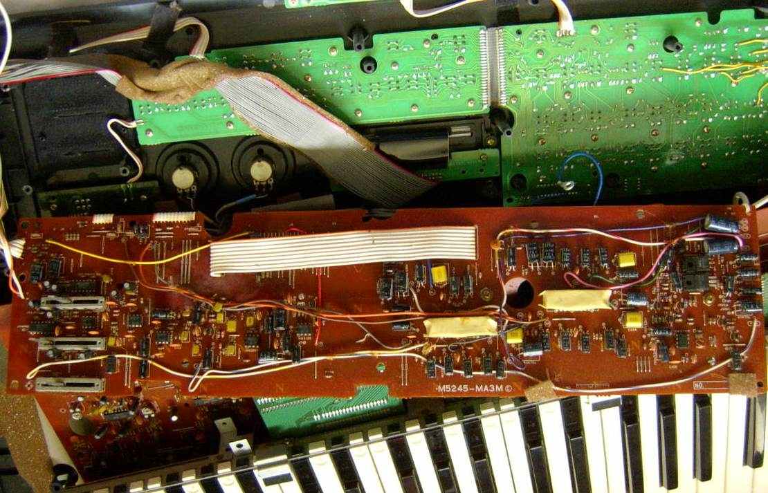
The circuitry is spread across 4 large and some smaller PCBs, those
include plenty of analogue stuff.
The HT-6000 uses 4 sound ICs D935G those are each driving 2 VCA. It
does not use the dedicated squarewave bass channel, because it layers the
outputs from each 2 sound ICs for upper and lower (chord) keyboard section
and so uses one of the melody channels as bass. The LCD is operated by
sound IC 1(all pins) and 2 (omitting pins 26..28).
Gate Array A (NEC D65012G197) handles
the address decoding of CPU pins A12..A15 for ROM, RAM, RAM-Card, 3 percussion
ICs and LED matrix. ROM1 is selected directly by A15.
ROM1 = program rom
ROM2 = preset voice/rhythm pattern data
RAM1 = system's work area
RAM2 = user voice/rhythm pattern data of internal memory
Gate Array B (NEC D65006G186) handles
address decoding of CPU pins A6..A11 to the 4 SD sound ICs, key cpu input
to the data bus and produces 3 clock frequencies (CK1=10MHz, CK2=2.5MHz,
CK3=250 kHz).
service mode
To enter test mode, hold 'Upper Tone 1'..'3' buttons and press 'Chord Off'.
The display will show "CASIO", "HT6000" (the "T" looks
like a mirrored "7"). If address lines are not ok it indicates "HT-FAIL".
If RAMs is bad it shows "FAIL" (else "Good"). Then all
LCD segments are lit (4 arrows + "88888888"). Finally the CPU
shuts power off to test APO.
For VCF adjustment mode hold 'Upper Tone 1'..'3' buttons and press 'Split'.
It will display "Fcut 0". This is nothing saved to flash memory.
You need to connect a scope to each 2090D
VCF IC to compare wafeform voltages on pins and turn trimmers. Polyphonic
analogue instruments are more complicated, so this is usefull if anybody
fucked up the trimmers during experimentation causing channel timbres to
differ. The bias voltage is common for all polyphony channels, but cutoff
has 8 individual trimmers.
| My Casio HT-6000 service manual PDF is a mess of partial page fragments.
I hope I sorted the puzzle correctly. The text apparently says:
VCF Adjustments
To execute VCF Adjustment mode program, press Upper Tone 1, 2, 3 switches
simultaneously and then press "SPLIT" button.
VCF Bias Voltage Adjustment
1.) By the above operation, the display shows: "Fcut 0".
2.) Adjust variable resistor VR17 on PCB M5245-MA2M so that the voltage
on VCF 1 (NJM-2090-1) pin 3 (checkpoint A1) is 2.00V +/-2mV.
3.) Make sure that pin 3 voltages of VCF 2 (NJM-2090-2) ~ VCF 8 (NJM-2090-8)
are within 2.00V +/-15mV.
VCF Cutoff Frequency Adjustment
1.) Sequentially from VCF bias voltage adjustment, press CHORD "ON"
button. Display then indicates: "Fcut 1".
For VCF bias voltage adjustment now press "Chord On" button. It will
display "Fcut 1".
2.) Music LSIs provide the following voltages and waveforms to corresponding
VCF pins.
OP OUT (pin 3) = DC 0.5~0.6V
VQC (pin 9) = DC 0.5~0.6V
IN (pin 18) = 640Hz 0.46~0.52 Vrms sine wave
3.) Connecting an oscilloscope to pin 12 of a VCF (NJM-2090), check
the peak to peak voltage of the waveform.
4.) Press CHORD "FINGERED" button. The LCD indicates "Fcut 2".
5.) Music LSIs provide the following voltages and waveforms to corresponding
VCF pins.
OP OUT (pin 3) = DC 2V
VQC (pin 9) = DC 0.5~0.6V
IN (pin 18) = 640Hz 0.46~0.52 Vrms sine wave
6.) Observing VCF's pin 12 waveform. Turn cutoff frequency adjustment
VRs (VR3, VR4, VR7, VR8, VR11, VR15 and VR16) so that peak to peak voltage
of the waveform is 1/4 of the formerly checked voltage in the above procedure
3.
7.) Perform the above procedures 1~6 for all the VCFs." |
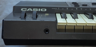
keyboard matrix
Because the keyboard is velocity sensitive, it uses 2 rows of contacts
to precisely measure the timing interval between upper and lower contact
when they close. Therefore the keyboard matrix is read by a separate Key
CPU "NEC D80C49HC 187" that communicates with the main CPU and controls
the key touch controller IC M6200,
which contains RC circuits and 5-bit DAC. The KI# inputs here are analogue
to sense the mixed signal of both contacts from a key (KC#A and KC#B) simultaneously.
This wiring is 1:1 identical with Casio
CT-6000 beside the omitted aftertouch mechanism.
The keys are sorted (left to right) from KI38 to KI8 with each line
alternatingly to KC2X, KC1X. This pattern exists twice with "X" being "A"
(upper contact) or "B" (lower contact). So the leftmost keys low contacts
begin with 'C1(2)' KC2B->KI38, 'C#1(2)' KC1B->KI38, 'D1(2)' KC2B->KI37,
'D#1(2)' KC1B->KI37 etc. and end with 'C6(2)' KC2B->KI8.
The panel matrix is scanned by the CPU signals PA0..PA3 through decoder
TC74HC154 for KC# outputs. The KI# inputs and data from the Key CPU are
muxed by gate array B on the data bus.
I haven't analyzed this matrix by myself, so there may be unknown eastereggs.
|
KI0
|
KI1
|
KI2
|
KI3
|
KI4
|
KI5
|
KI6
|
KI7
|
|
pin
|
|
in 0
|
in 1
|
in 2
|
in 3
|
in 4
|
in 5
|
in 6
|
in 7
|
in / out
|
|
O.
synth. ens.
|
O.
cosmic dance
|
O.
string ens.
|
O.
brass ens.
|
O.
pipe organ
|
|
line 1
|
line 1
|
out 0
|
KC0
|
O.
piano
|
O.
harpsichord
|
O.
guitar
|
O.
trumpet
|
O.
vibraphone
|
O.
select
|
line 2
|
line 2
|
out 1
|
KC1
|
OL.
synth ens.
|
OL.
brass ens.
|
OL.
synth. brass
|
OL.
cosmic dance
|
OL.
jazz organ
|
OL.
bass/ obligato
|
line 3
|
line 3
|
out 2
|
KC2
|
OL.
piano
|
OL.
harpsichord
|
OL.
harp
|
OL.
guitar
|
OL.
synth. guitar
|
C.
accomp. variation
|
|
|
out 3
|
KC3
|
R.
rock
|
R.
8 beat
|
R.
16 beat
|
R.
disco
|
R.
pops
|
R.
variation
|
line 4
|
line 4
|
out 4
|
KC4
|
R.
swing
|
R.
slow rock
|
R.
samba
|
R.
bossa nova
|
R.
waltz
|
R.
preset A
|
|
detune
|
out 5
|
KC5
|
OL.
preset
|
OL.
internal
|
OL.
card
|
|
|
R.
preset B
|
velocity
|
amplitude level
|
out 6
|
KC6
|
O.
preset
|
O.
internal
|
O.
card
|
C.
auto harmonize
|
|
|
O.
edit
|
OL. edit
|
out 7
|
KC7
|
R.
internal
|
R.
card
|
|
|
|
|
pattern/ midi
|
write
|
out 8
|
KC8
|
|
|
|
R.
intro/ ending
|
S.
chord mem. record/ delete
|
S.
op. mem. record
|
S.
chord/ op. mem. select
|
R.
synchro/ fill-in
|
start/stop.
|
out 9
|
KC9
|
|
|
|
|
|
C.
normal
|
C.
split
|
C.
fingered
|
C.
single finger
|
out 10
|
KC10
|
The input lines are active-low, i.e. react on GND. Any functions can
be triggered by a non- locking switch in series to a diode from one "in"
to one "out" pin.
legend:
|
|
|
underlined
|
= function needs locking switch (i.e. stays active only so long the
switch is closed) |
|
R.
|
= preset rhythm |
|
O.
|
= preset sound upper keys ('orchestra') |
|
OL.
|
= preset sound lower keys |
|
C.
|
= chord |
|
S.
|
= sequencer |
orange
background |
= easteregg (unconnected feature) |
grey
background |
= unconnected doublet |
The panel LEDs are latched through gate array A from the data bus.
pinout D80C49HC-187
The "NEC D80C49HC 187" is the Key CPU of Casio CT-6000. It sits between
keys velocity controller OKI M6200 and main CPU to speed up communication.
Technically it is an Intel MC-48 MCU with internal ROM.
| pin |
name |
purpose |
| 1 |
T0 |
data clock in |
| 2 |
XTAL1 |
clock in (8.96 MHz) |
| 3 |
XTAL2 |
(not used) |
| 4 |
/RESET |
reset |
| 5 |
/SS |
|
| 6 |
/INT |
interrupt in (from velocity ic) |
| 7 |
EA |
|
| 8 |
/RD |
read enable out (to velocity ic) |
| 9 |
/PSEN |
|
| 10 |
/WR |
write enable out (to velocity ic) |
| 11 |
ALE |
address latch enable out (to velocity ic) |
| 12 |
DB0 |
data bus (for velocity ic) |
| 13 |
DB1 |
data bus (for velocity ic) |
| 14 |
DB2 |
data bus (for velocity ic) |
| 15 |
DB3 |
data bus (for velocity ic) |
| 16 |
DB4 |
data bus (for velocity ic) |
| 17 |
DB5 |
data bus (for velocity ic) |
| 18 |
DB6 |
data bus (for velocity ic) |
| 19 |
DB7 |
data bus (for velocity ic) |
| 20 |
Vss |
ground 0V |
| 21 |
P20 |
(not used) |
| 22 |
P"1 |
(not used) |
| 23 |
P22 |
(not used) |
| 24 |
P23 |
(not used) |
| 25 |
PROG |
(not used) |
| 26 |
VDD /STOP |
supply voltage +5V |
| 27 |
P10 |
data bus D0 |
| 28 |
P11 |
data bus D1 |
| 29 |
P12 |
data bus D2 |
| 30 |
P13 |
data bus D3 |
| 31 |
P14 |
data bus D4 |
| 32 |
P15 |
data bus D5 |
| 33 |
P16 |
data bus D6 |
| 34 |
P17 |
data bus D7 |
| 35 |
P24 |
(not used) |
| 36 |
P25 (CNT49) |
control signal in (from cpu) |
| 37 |
P26 (INT49) |
interrupt out (to cpu) |
| 38 |
P27 (WR49) |
data timing pulse out |
| 39 |
T1 (TST) |
test /in |
| 40 |
VCC |
supply voltage +5V |
pinout D78C10G
The CPU "NEC D78C10G" (64 pin zigzag DIL) was used in Casio SD synthesizers.
It is a documented romless 8-bit microcontroller, which behaviour depends
on software in external rom. It has 256 byte internal RAM.
This is the pin meaning when used in Casio HT-6000, which substancially
differs from HT-3000
hardware family.
| pin |
name |
CPU pin |
purpose |
| 1 |
PA0 |
|
key matrix mux in |
| 2 |
PA1 |
|
key matrix mux in |
| 3 |
PA2 |
|
key matrix mux in |
| 4 |
PA3 |
|
key matrix mux in |
| 5 |
PA4 |
|
address for rom2 |
| 6 |
PA5 |
|
address for rom2 |
| 7 |
PA6 |
|
address for rom2 |
| 8 |
PA7 |
|
? |
| 9 |
PB0 |
|
stereo chorus enable out |
| 10 |
PB1 |
|
stereo chorus depth out (hi=deep) |
| 11 |
PB2 |
|
(not used) |
| 12 |
PB3 |
|
(not used) |
| 13 |
PB4 |
|
(not used) |
| 14 |
PB5 |
|
ram card read /enable out |
| 15 |
PB6 |
|
ram card write /enable out |
| 16 |
PB7 |
|
ram card detect /in |
| 17 |
MOS |
PC0/TXD |
midi out |
| 18 |
PC1 |
PC1/RXD |
midi out |
| 19 |
N |
PC2/SCK |
melody /accomp. changeover out |
| 20 |
PC3 |
PC3/ /INT2 |
key cpu irq in |
| 21 |
PC4 |
PC4/TO |
key cpu control in |
| 22 |
PC5 |
PC5/CI |
key cpu data request in |
| 23 |
PC6 |
PC6/CO0 |
(not used) |
| 24 |
APO |
PC7/CO1 |
auto-power-off /out |
| 25 |
OFF |
/NMI |
power-off /in |
| 26 |
DWN |
INT1 |
low battery voltage /detect in |
| 27 |
MODE1 |
|
(wired through 22k to VDD) |
| 28 |
/RESET |
|
reset |
| 29 |
MODE0 |
|
(wired through 22k to VDD) |
| 30 |
X2 |
|
crystal out |
| 31 |
X1 |
|
crystal in (12 MHz) |
| 32 |
VSS |
|
ground 0V |
|
|
| pin |
name |
CPU pin |
purpose |
| 33 |
AVSS |
|
port T threshold voltage in (ADC ground) |
| 34 |
AN0 |
|
analogue in (not used) |
| 35 |
AN1 |
|
pitch wheel in |
| 36 |
AN2 |
|
modulation wheel in |
| 37 |
AN3 |
|
low battery voltage sense in |
| 38 |
AN4 |
|
analogue in (not used) |
| 39 |
AN5 |
|
entry dial in |
| 40 |
AN6 |
|
analogue in (not used) |
| 41 |
AN7 |
|
analogue in (not used) |
| 42 |
VAref |
|
ADC reference voltage |
| 43 |
AVCC |
|
ADC supply voltage +5V |
| 44 |
/RD |
|
read strobe out |
| 45 |
/WR |
|
write strobe out |
| 46 |
ALE |
|
address latch out |
| 47 |
A8 |
PF0 |
port F I/O | address bus bit 8 |
| 48 |
A9 |
PF1 |
port F I/O | address bus bit 9 |
| 49 |
A10 |
PF2 |
port F I/O | address bus bit 10 |
| 50 |
A11 |
PF3 |
port F I/O | address bus bit 11 |
| 51 |
A12 |
PF4 |
port F I/O | address bus bit 12 |
| 52 |
A13 |
PF5 |
port F I/O | address bus bit 13 |
| 53 |
A14 |
PF6 |
port F I/O | address bus bit 14 |
| 54 |
A15 |
PF7 |
port F I/O | address bus bit 15 |
| 55 |
D0 |
PD0 |
port D I/O | address / data bus |
| 56 |
D1 |
PD1 |
port D I/O | address / data bus |
| 57 |
D2 |
PD2 |
port D I/O | address / data bus |
| 58 |
D3 |
PD3 |
port D I/O | address / data bus |
| 59 |
D4 |
PD4 |
port D I/O | address / data bus |
| 60 |
D5 |
PD5 |
port D I/O | address / data bus |
| 61 |
D6 |
PD6 |
port D I/O | address / data bus |
| 62 |
D7 |
PD7 |
port D I/O | address / data bus |
| 63 |
VDD |
|
RAM backup power supply | /stop (wired to VCC) |
| 64 |
VCC |
|
supply voltage +5V |
|
pinout D65012G197
The "NEC D65012G197" (80 pin SMD) is the Gate Array A of Casio HT-6000.
It handles the address decoding of CPU pins A12..A15 for ROM, RAM, RAM-Card,
3 percussion ICs and LED matrix. ROM1 is selected directly by A15. Rise
of ALE latches databus into lower address bus (A0..A7).
| pin |
name |
purpose |
| 1 |
/RST |
reset |
| 2 |
LD7 |
led out |
| 3 |
LD5 |
led out |
| 4 |
LD5 |
led out |
| 5 |
LD4 |
led out |
| 6 |
LD3 |
led out |
| 7 |
LD1 |
led out |
| 8 |
LD0 |
led out |
| 9 |
LC1 |
led matrix out |
| 10 |
LC3 |
led matrix out |
| 11 |
LC0 |
led matrix out |
| 12 |
GND |
ground 0V |
| 13 |
GND |
ground 0V |
| 14 |
LS0 |
led matrix out |
| 15 |
LS1 |
led matrix out |
| 16 |
LS2 |
led matrix out |
| 17 |
LS3 |
led matrix out |
| 18 |
LS4 |
led matrix out |
| 19 |
LS5 |
led matrix out |
| 20 |
LS6 |
led matrix out |
| 21 |
LS7 |
led matrix out |
| 22 |
LC6 |
led matrix out |
| 23 |
LC5 |
led matrix out |
| 24 |
LC4 |
led matrix out |
| 25 |
B12 |
ram card address out |
| 26 |
B7 |
ram card address out |
| 27 |
B6 |
ram card address out |
| 28 |
B5 |
ram card address out |
| 29 |
B4 |
ram card address out |
| 30 |
B3 |
ram card address out |
| 31 |
B2 |
ram card address out |
| 32 |
B1 |
ram card address out |
| 33 |
GND |
ground 0V |
| 34 |
VDD |
supply voltage 5V |
| 35 |
B0 |
ram card address out |
| 36 |
/CE |
chip enable |
| 37 |
B10 |
ram card address out |
| 38 |
B11 |
ram card address out |
| 39 |
B5 |
ram card address out |
| 40 |
B6 |
ram card address out |
|
|
| pin |
name |
purpose |
| 41 |
D3 |
data bus in |
| 42 |
D2 |
data bus in |
| 43 |
D4 |
data bus in |
| 44 |
D1 |
data bus in |
| 45 |
D5 |
data bus in |
| 46 |
D0 |
data bus in |
| 47 |
D6 |
data bus in |
| 48 |
D7 |
data bus in |
| 49 |
A0 |
address bus out |
| 50 |
A1 |
address bus out |
| 51 |
BK |
rom2 chip select out |
| 52 |
A2 |
address bus out |
| 53 |
GND |
ground 0V |
| 54 |
A10 |
address bus in |
| 55 |
A3 |
address bus out |
| 56 |
A4 |
address bus out |
| 57 |
A11 |
address bus in |
| 58 |
A5 |
address bus out |
| 59 |
A9 |
address bus in |
| 60 |
A6 |
address bus out |
| 61 |
A8 |
address bus in |
| 62 |
A7 |
address bus out |
| 63 |
A13 |
address bus in |
| 64 |
A14 |
address bus in |
| 65 |
A15 |
address bus in |
| 66 |
A12 |
address bus in |
| 67 |
RCSB |
RCSA ram chip select out |
| 68 |
RCSA |
RCSB ram chip select out |
| 69 |
CE |
chip enable |
| 70 |
/RD |
read enable |
| 71 |
GND |
ground 0V |
| 72 |
VDD |
supply voltage 5V |
| 73 |
ALE |
address latch enable in |
| 74 |
/WR |
write enable |
| 75 |
C0 |
percussion ic1 chip select out |
| 76 |
C1 |
percussion ic2 chip select out |
| 77 |
C2 |
percussion ic2 chip select out |
| 78 |
C6 |
gate array B data select out |
| 79 |
C7 |
gate array B data select out |
| 80 |
C5 |
gate array B data select out(?) |
|
In schematics, pin 67 RCSB and 68 RCSA wires are swapped.
pinout D65006G186
The "NEC D65006G186" (64 pin SMD) is the Gate Array B of Casio HT-6000.
It handles address decoding of CPU pins A6..A11 to the 4 SD sound ICs,
key cpu input to the data bus and produces 3 clock frequencies (CK1=10MHz,
CK2=2.5MHz, CK3=250 kHz).
| pin |
name |
purpose |
| 1 |
NC |
(not used) |
| 2 |
XT2 |
crystal out |
| 3 |
XT1 |
crystal in (10 MHz) |
| 4 |
CK1 |
key cpu clock out (10 MHz) |
| 5 |
TST |
test (wired to ground 0V) |
| 6 |
T0 |
key cpu data enable out |
| 7 |
/RST |
reset |
| 8 |
KI0 |
keyboard matrix in |
| 9 |
KI1 |
keyboard matrix in |
| 10 |
KI2 |
keyboard matrix in |
| 11 |
KI3 |
keyboard matrix in |
| 12 |
KI4 |
keyboard matrix in |
| 13 |
KI5 |
keyboard matrix in |
| 14 |
KI6 |
keyboard matrix in |
| 15 |
KI7 |
keyboard matrix in |
| 16 |
C5 |
gate array A data select in(?) |
| 17 |
C7 |
gate array A data select in |
| 18 |
C6 |
gate array A data select in |
| 19 |
/WR |
write enable in |
| 20 |
CK3 |
percussion ic clock out (250 kHz) |
| 21 |
A11 |
address bus in |
| 22 |
A10 |
address bus in |
| 23 |
A9 |
address bus in |
| 24 |
A8 |
address bus in |
| 25 |
A7 |
address bus in |
| 26 |
GND |
ground 0V |
| 27 |
VDD |
supply voltage 5V |
| 28 |
A6 |
address bus in |
| 29 |
D7 |
data bus |
| 30 |
D6 |
data bus |
| 31 |
D5 |
data bus |
| 32 |
D4 |
data bus |
|
|
| pin |
name |
purpose |
| 33 |
D3 |
data bus |
| 34 |
D2 |
data bus |
| 35 |
D1 |
data bus |
| 36 |
D0 |
data bus |
| 37 |
/CS0 |
sound ic1 chip select out |
| 38 |
/CS1 |
sound ic2 chip select out |
| 39 |
/CS2 |
sound ic3 chip select out |
| 40 |
/CS3 |
sound ic4 chip select out |
| 41 |
DS7 |
sound ic data out |
| 42 |
DS6 |
sound ic data out |
| 43 |
DS5 |
sound ic data out |
| 44 |
DS4 |
sound ic data out |
| 45 |
DS3 |
sound ic data out |
| 46 |
DS2 |
sound ic data out |
| 47 |
DS1 |
sound ic data out |
| 48 |
DS0 |
sound ic data out |
| 49 |
/I2 |
sound ic data read out |
| 50 |
/I1 |
sound ic command read out |
| 51 |
/WRS |
sound ic write enable out |
| 52 |
CK2 |
velocity ic clock out (2.5 MHz) |
| 53 |
P10 |
key cpu data in |
| 54 |
P11 |
key cpu data in |
| 55 |
P12 |
key cpu data in |
| 56 |
P13 |
key cpu data in |
| 57 |
VDD |
supply voltage 5V |
| 58 |
GND |
ground 0V |
| 59 |
GND |
ground 0V |
| 60 |
P14 |
key cpu data in |
| 61 |
P15 |
key cpu data in |
| 62 |
P16 |
key cpu data in |
| 63 |
P17 |
key cpu data in |
| 64 |
P27 |
key cpu data timing in |
|
|